


All Products
Contact Person :
Hang Ning
Phone Number :
+86 15009270259
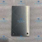
Feiteng 200*120*8mm Hafnium Sheet High Temp Resistant


| Place of Origin | Baoji, Shaanxi, China |
|---|---|
| Brand Name | Feiteng |
| Certification | GB/T19001-2016 idt ISO9001:2015; GJB9001C-2017 |
| Model Number | Hafnium plate |
| Minimum Order Quantity | To be negotiated |
| Price | To be negotiated |
| Packaging Details | Wooden case |
| Delivery Time | To be negotiated |
| Payment Terms | T/T |
| Supply Ability | To be negotiated |
Product Details
| Brand Name | Feiteng | Model Number | Hafnium Plate |
|---|---|---|---|
| Certification | GB/T19001-2016 Idt ISO9001:2015; GJB9001C-2017 | Size | 200*120*8 |
| Place Of Origin | Baoji, Shaanxi, China | ||
| Highlight | 200*120*8mm Hafnium Sheet,Feiteng Hafnium Sheet,Hafnium Plate High Temp Resistant |
||
Product Description
Hafnium Plate 200*120*8 Hafnium Sheet
| Item name | Hafnium plate |
| Packaging | Custom |
| Size | 200*120*8 |
| Port of place | Xi'an port, Beijing port, Shanghai port, Guangzhou port, Shenzhen port |
Hafnium is a metallic element, symbol Hf, atomic number 72, atomic weight 178.49. Elemental is a lustrous silver-gray transition metal. There are six naturally stable isotopes of hafnium: hafnium 174, 176, 177, 178, 179, 180. Hafnium does not react with dilute hydrochloric acid, dilute sulfuric acid and strong alkali solutions, but is soluble in hydrofluoric acid and aqua regia. The element name comes from the Latin name for the city of Copenhagen. Swedish chemist Hewei xi and Dutch physicist Kest in 1925 with the method of fluoride salt classification crystallization of hafnium salt, and metal sodium reduction, to get pure metal hafnium. Hafnium is found in 0.00045% of the earth's crust and is often associated with zirconium in nature. The element hafnium is also used in the latest intel45 nm processors. Because of the Manufacturability of SiO2 and its ability to reduce the thickness for continuous improvement of transistor performance, processor manufacturers are using SiO2 as the gate dielectric material. When Intel import 65 nano manufacturing technology, has been to cut silica gate dielectric thickness to 1.2 nm, the equivalent of five layers of atoms, but due to the size of the transistor to atomic size, power consumption and heat dissipation difficulty will increase at the same time, an electrical current waste and unnecessary heat, so if continue to use current material, further reducing thickness, The leakage rate of the gate dielectric will increase significantly, which will limit the technology of shrinking transistors. To address this critical problem, Intel is planning to switch to a thicker, high-K material (hafnium-based material) as the gate dielectric, replacing silicon dioxide, which has also reduced leakage by more than 10 times. Intel's 45-nanometer process nearly doubles the density of transistors compared to its 65-nanometer predecessor, increasing the number of transistors on the processor or reducing the size of the processor. In addition, transistors require less power to switch on and off, using nearly 30% less power. Interconnects use copper wires with low-K dielectrics. Smoothly improve the efficiency and reduce the power consumption, switch speed up about 20%.
Features:
plasticity
Easy processing
High temperature resistant
Corrosion resistant
Recommended Products